|
Due date: On or before Monday, April 22, 2024 Absolutely no copying others’ works |
Name: _______________________ |
- Upload the completed homework to the section of “COVID-19 Exams, Homeworks, & Programming Exercises” of Blackboard.
- The purpose of homeworks is for students to practice for the exams without others’ help, so the penalty of mistakes will be minor.
- Without practicing for the exams properly, students would not be able to do well on the exams.
- Consider the following instruction mix:
R-type I-type (non- lw)Load Store Branch Jump 15% 30% 25% 10% 15% 5%
- (10%) What fraction of all instructions use data memory?
Ans> - (10%) What fraction of all instructions use instruction memory?
Ans> - (10%) What fraction of all instructions use the sign extend (SE)?
Ans> - (10%) What is the sign extend doing during cycles in which its output is not needed?
Ans>
- (10%) What fraction of all instructions use data memory?
- In this exercise we examine in detail how an instruction is executed in a single-cycle datapath.
Use the slides, NOT textbook, to answer the following questions, especially the Slide 12.10 and 12.13 figures as follows:
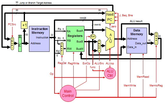
Problems in this exercise refer to a clock cycle in which the processor fetches the following instruction word:0001 0000 0010 0011 0000 0000 0000 1100
Check the Appendix A.10 of the textbook to find out what this instruction is. Assume that data memory is all zeros and that the processor’s registers have the following values at the beginning of the cycle in which the above instruction word is fetched:
$0$1$2$3$4$5$6$8$12$310 10 -5 8 -1 20 4 -4 15 -10
- (10%) What are the values of ALU control unit’s inputs for this instruction (the ALU control unit is shown in the figure of Slide 12.12)?
Ans> - (14%)
What is the new PC address after this instruction is executed?
Specify all paths through which this value is determined.
†Hint: Use PC to represent the program counter or its content (a bit string).
Ans>- New PC (30 bits) =
-
Path 1: PC ⇒
Path 2: PC ⇒
...
- (10%) What are the values of ALU control unit’s inputs for this instruction (the ALU control unit is shown in the figure of Slide 12.12)?
- (12%) For each mux, show the values of its inputs and outputs during the execution of this instruction.
†Hint:
- Use PC to represent the program counter or its content (a bit string).
- If the control signal for a mux is X (don’t care), show both output values for control signal values 0 and 1.
- The default value for a register number is 0.
- The memory content at the address,
addr, isMem[addr].
- WrReg Mux (
RegDst):- Inputs:
- Output:
- ALU Mux (
ALUSrc):- Inputs:
- Output:
- Mem/ALU Mux (
MemtoReg):- Inputs:
- Output:
- Jump Mux (
J) (30 bits):- Inputs:
- Output:
- PC Mux (
PCSrc) (30 bits):- Inputs:
- Output:
- (12%) What are the input values for the ALU and the two add units?
†Hint: Use PC to represent the program counter or its content (a bit string).
Ans>- ALU:
- Add (PC+1) (30 bits):
- Add (Branch) (30 bits):
- (12%) What are the values of all inputs for the registers unit?
†Hint:- The answer could be X (don’t care).
- The default value for a register number is 0.
- Read Register 1 (RA):
- Read Register 2 (RB):
- Write Register (RW):
- Write Data (BusW):
- RegWrite: