Chip Manufacturing Process


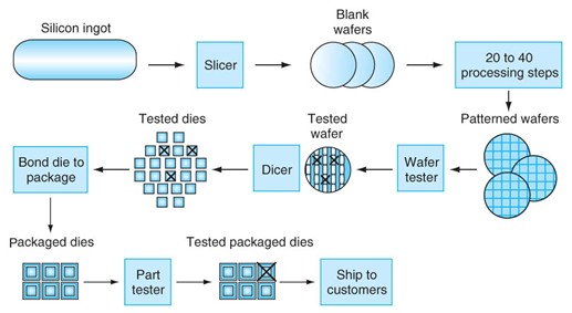
The manufacturing process of integrated circuit takes the following steps:

  1. It starts with a silicon crystal ingot, which looks like a giant sausage. Today, ingots are 8-12 inches in diameter and about 12-24 inches long.


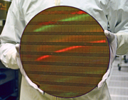
  1. An ingot is finely sliced into wafers no more than 0.1 inch thick. A wafer is then used to created chips.
  1. These wafers then go through a series of processing steps, during which patterns of chemicals are placed on each wafer, creating one layer of transistors and two to eight levels of conductors, separated by layers of insulators.

  2. These patterned wafers are then tested with a wafer tester, and a map of the good parts is made.
  1. Then, the wafers are diced into dies or chips, each of which is the individual rectangular sections. Dicing enables you to discard only those dies that contain the flaws, rather than the whole wafer.

  2. The yield is the percentage of good dies from the total number of dies on the wafer. In the previous figure, one wafer produced 20 dies, of which 17 passed testing. (X means the die is bad.) The yield of good dies in this case was 17/20, or 85%.

  3. These good dies are then bonded into packages and tested one more time before shipping the packaged parts to customers. One bad packaged part was found in this final test.
Review: IC (Integrated Circuit)
    If one wafer produced 25 dies, of which 20 passed testing. What is the yield of good dies?

      0.2
      0.4
      0.8
      0.9
Result:        


      Kevin says he was completely in the dark    
      about the CEO’s plans to sell the company.